As the backbone of modern electronics, printing circuit boards (PCBs) play a pivotal role in a multitude of devices, from smartphones to sophisticated medical equipment. According to the market research firm Grand View Research, the global PCB market is expected to reach USD 100.2 billion by 2025, reflecting a compound annual growth rate (CAGR) of 3.5%. This burgeoning industry presents significant opportunities for newcomers looking to delve into PCB design and manufacturing. However, the intricacies involved in creating functional and reliable PCBs can be daunting for beginners. This comprehensive guide aims to demystify the process of printing circuit boards, providing essential insights, techniques, and tips necessary for aspiring engineers and hobbyists alike to successfully navigate the world of PCB creation. By understanding the fundamental principles and incorporating best practices, individuals can unlock the secrets to producing high-quality circuit boards that meet the demands of today's technology-driven market.
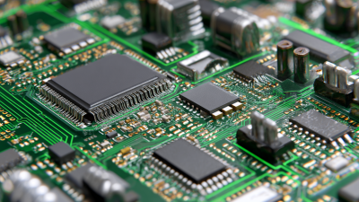
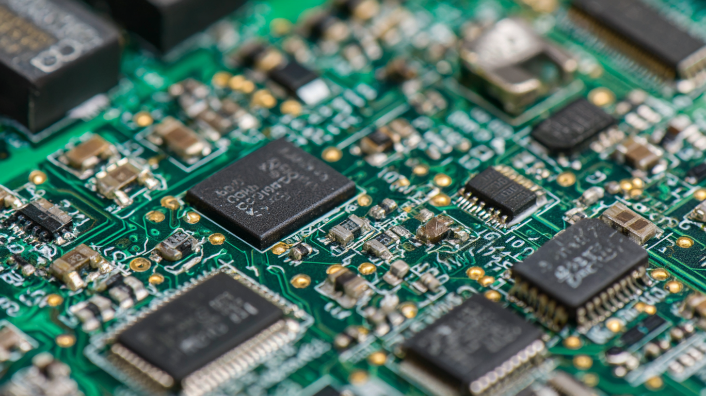
Printed Circuit Boards (PCBs) form the backbone of modern electronic devices, providing essential structural and electrical connections. Understanding the basics of PCBs involves grasping key concepts such as substrate materials, layer configuration, and manufacturing processes. As the demand for high precision in electronic applications grows, considerations like temperature sensitivity have become pivotal. In recent designs, particularly in wearable temperature sensors, addressing issues related to thermal, electrical, and mechanical aspects is crucial for achieving accuracy within ±0.1°C.
Moreover, the semiconductor packaging substrate industry is witnessing profound developments. The manufacturing processes encompass several stages, including wafer fabrication and substrate assembly, which ultimately influence the performance and reliability of PCBs. According to a deep dive into the semiconductor packaging market, innovations in soft and rigid circuit designs are reshaping how PCBs are integrated into compact devices. With industry projections indicating significant upticks in PCB concept stocks, understanding the interconnectedness of the PCB supply chain—from hard boards to flexible circuits—will be paramount for both newcomers and seasoned professionals in the field.
When embarking on the journey of PCB design and production, having the right tools and materials is instrumental for beginners. According to the IPC (Institute of Printed Circuits), the global PCB market is expected to reach $75.9 billion by 2025, highlighting the growing demand for efficient and innovative PCB solutions. This surge necessitates a foundational understanding of the essential components integral to PCB manufacturing.
Beginner PCB designers should equip themselves with software tools like Eagle, Altium Designer, or KiCAD, which facilitate schematic capture and PCB layout design. These tools not only streamline the design process but also provide libraries of predefined components, crucial for minimizing the risk of errors. Additionally, a basic understanding of materials such as FR-4 (a common epoxy fiberglass) and HDI (High-Density Interconnect) can significantly impact the quality and performance of the final product. Research indicates that approximately 50% of PCB failures stem from material selection, emphasizing the importance of using high-quality substrates in the design process. By mastering these tools and materials, beginners can effectively transition from conceptualization to production, paving the way for successful PCB projects.
Designing your first PCB layout can be an exciting yet daunting task, especially for beginners. With the rapid advancements in Electronic Design Automation (EDA) tools, the process has become significantly more accessible. These software solutions simplify the intricacies of PCB design by providing user-friendly interfaces and automated features that guide you through each stage of the design process. From schematic capture to layout, modern EDA tools enhance productivity and reduce development time, allowing novice designers to achieve professional results more quickly.
As you embark on your PCB layout journey, it's essential to understand the fundamental steps involved. Start by defining your project requirements and selecting the right components. Then, create a schematic diagram that logically represents the connections between different parts. With the schematic in place, you can proceed to layout your PCB, ensuring that components are placed efficiently and that traces are routed correctly to minimize interference and optimize signal integrity. Utilizing integrated tools that include real-time design rule checks will help you identify potential errors early in the process, paving the way for a successful first PCB.
Printed Circuit Boards (PCBs) are integral to modern electronics, yet beginners often face several challenges during the manufacturing process. One common issue is design complexity, where intricate layouts can lead to errors in component placement and trace routing. To overcome this, beginners should invest time in learning PCB design software and utilize automated design rule checks that highlight potential mistakes before production begins. This proactive approach minimizes errors and ensures a more reliable final product.
Another significant challenge is material selection. Different projects require different types of substrates, copper weights, and laminate materials. Inadequate understanding of these materials can lead to issues like thermal performance problems or electromagnetic interference. Beginners should educate themselves on various materials and their properties, considering the specific needs of their projects. Partnering with experienced manufacturers can also provide valuable insights, ensuring that the selected materials meet both the technical requirements and budget constraints. By addressing these common pitfalls head-on, newcomers can streamline their PCB manufacturing process and achieve better outcomes.
The landscape of printed circuit board (PCB) manufacturing has evolved dramatically with the advent of innovative techniques and technologies. In the realm of PCB printing, advancements such as digital printing and additive manufacturing have transformed traditional approaches. Digital printing allows for the rapid prototyping of PCBs, enabling designers to produce complex circuits with shorter lead times and at a fraction of the cost of conventional methods. This technology significantly enhances design flexibility, making it easier for engineers to iterate and optimize their creations before moving to mass production.
Furthermore, the integration of advanced materials, like flexible substrates and nanomaterials, is enhancing the performance and durability of PCBs. These materials enable the production of lighter, more efficient circuits that can operate under a range of conditions. Innovations in soldering techniques, such as laser soldering and selective soldering, are also streamlining assembly processes, reducing defects, and increasing yields. As these technologies continue to merge and evolve, they are setting new standards for quality and efficiency in PCB manufacturing, heralding a new era for both novices and seasoned professionals in the electronics industry.
| Technique | Description | Advantages | Applications | Future Trends |
|---|---|---|---|---|
| 3D Printing | Using additive manufacturing for PCB creation. | Rapid prototyping, customization potential. | Consumer electronics, IoT devices. | Integration with AI and smart materials. |
| Laser Etching | Using lasers to precisely etch patterns onto a substrate. | High precision, reduced waste. | Telecommunications, aerospace components. | Advancements in optical technology. |
| Subtractive Manufacturing | Carving circuit paths from a solid substrate material. | Established technique, availability of materials. | Traditional consumer electronics. | Automation in production processes. |
| Flexible PCBs | PCBs made with flexible materials. | Space-saving, lightweight. | Wearable technology, medical devices. | Integration with smart textiles. |
| High-Density Interconnect (HDI) | Technologies that allow for increased circuit density. | Maximized space usage, improved performance. | Smartphones, tablets, and laptops. | Continued miniaturization of electronics. |
MSIRobot