Understanding the Essentials of PCB Design and Assembly for Beginners
In the rapidly advancing world of electronics, a foundational understanding of PCB design and assembly is crucial for beginners looking to make their mark. This essential aspect of electronics involves creating printed circuit boards that serve as the backbone of virtually all electronic devices. Many newcomers often find themselves overwhelmed by the technical jargon and intricate processes involved in PCB design and assembly. However, grasping the fundamental concepts is not only achievable but vital for anyone aspiring to develop their skills in this field.
In this article, we will delve into the essential elements of PCB design and assembly, providing beginners with a clear roadmap to navigate the complexities of this discipline. By demystifying the process and highlighting key considerations, we aim to equip aspiring engineers and hobbyists with the knowledge they need to successfully embark on their PCB projects.
Key Principles of PCB Design: Essential Considerations for Beginners
When embarking on the journey of PCB design, beginners must grasp several key principles that lay the groundwork for effective and efficient assemblies. One of the essential considerations is the choice of materials used in the PCB. According to industry reports, the global printed circuit board market was valued at over $60 billion in 2021 and is projected to grow by more than 5% annually. This increase underscores the importance of selecting high-quality substrates, such as FR-4, which offer excellent electrical insulation and thermal stability.
Another critical aspect involves understanding the layout and routing of the PCB. Designers must ensure that the traces are adequately spaced to prevent signal interference, especially in high-frequency applications. The IPC-2221 standards provide guidelines on trace width and spacing, emphasizing that proper design can reduce EMI and enhance the overall performance and reliability of the circuit. Research shows that nearly 30% of PCB failures arise from design errors, illustrating the necessity for beginners to invest time in understanding these fundamental principles to avoid costly mistakes in their designs.
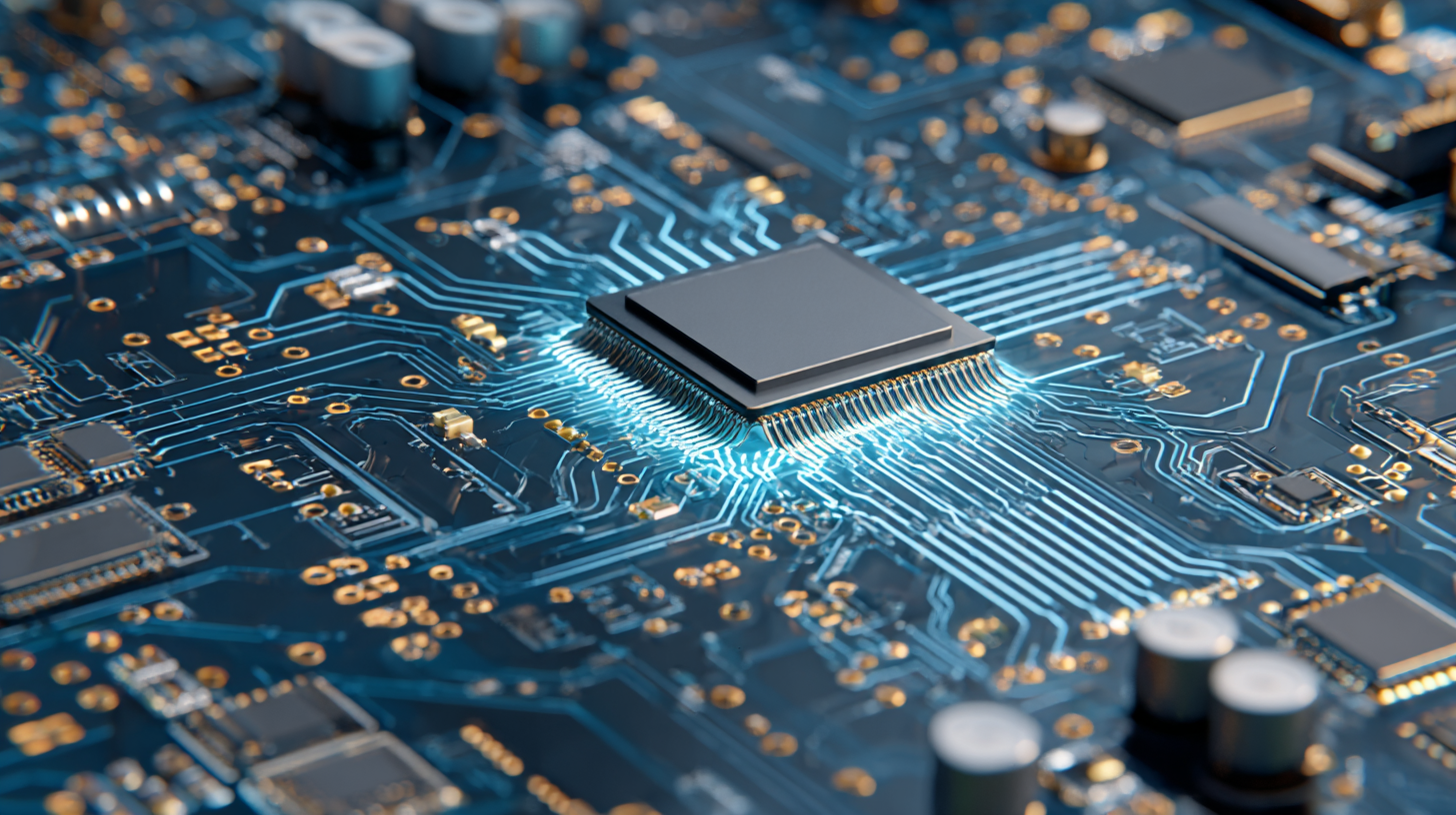
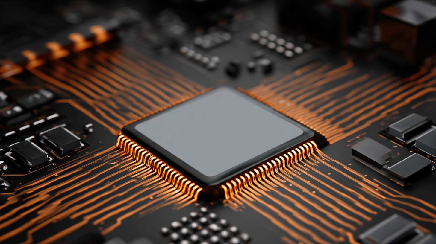
Understanding PCB Materials: Choosing the Right Substrate for Your Project
Choosing the right substrate is crucial in Printed Circuit Board (PCB) design, as it influences the performance and reliability of the final product. The most commonly used material is FR-4, which is a fiberglass-reinforced epoxy laminate. This material offers good electrical insulation and thermal stability, making it a versatile choice for most applications. However, depending on the project’s requirements, alternatives like PTFE or aluminum might be more suitable, especially in high-frequency or high-power applications.
When selecting a substrate, consider factors like dielectric constant, thermal conductivity, and mechanical strength. A lower dielectric constant can improve signal integrity for high-frequency circuits, while materials with higher thermal conductivity are essential for heat dissipation in power electronics. Ultimately, the right substrate not only ensures optimal circuit performance but also contributes to manufacturing efficiency and overall project cost-effectiveness.
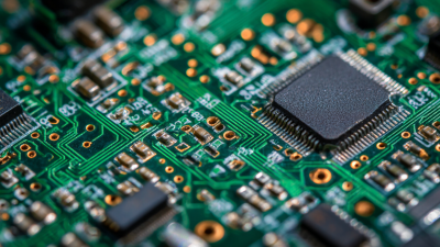
Common PCB Layout Techniques: Best Practices for Signal Integrity
When designing printed circuit boards (PCBs), achieving optimal signal integrity is crucial. One of the most effective techniques to enhance signal quality is proper trace routing. Designers should aim to keep traces as short as possible and avoid sharp angles to minimize impedance discontinuities. Additionally, using differential pairs for signals can significantly reduce electromagnetic interference, as they are routed closely together and effectively cancel out noise.
Another important aspect of PCB layout involves ground plane design. A solid ground plane helps to provide a low-resistance path for return currents, which is essential for minimizing noise and reducing voltage fluctuations. Furthermore, isolating sensitive components from noisy ones by strategically placing them on the board can improve overall performance. Utilizing vias—both blind and buried—can aid in managing the routing of high-frequency signals while keeping the layout clean and efficient. By adhering to these best practices, beginners can create PCBs that not only function well but also maintain signal integrity over time.
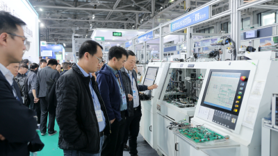
Assembly Processes: Exploring Methods for Efficient PCB Manufacturing
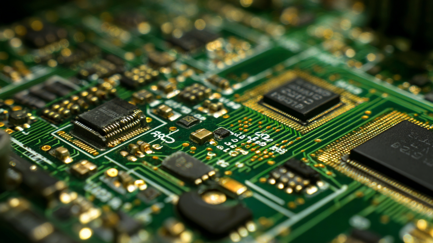
In the realm of PCB manufacturing, understanding assembly processes is crucial for efficiency and quality. One of the most common techniques used is Surface Mount Technology (SMT), where components are mounted directly onto the surface of the PCB. This method allows for higher density and more compact designs, significantly reducing the size and weight of electronic devices.
Automated pick-and-place machines facilitate this process, ensuring precision and minimizing human error. However, proper soldering techniques are vital to avoid issues such as cold joints or solder bridging.
Another essential assembly method is Through-Hole Technology (THT), which involves inserting component leads through drilled holes in the PCB and soldering them on the opposite side. While THT is generally considered more robust and better suited for high-stress applications, it is slower and can be more labor-intensive compared to SMT.
Hybrid assembly is also gaining popularity, combining both SMT and THT to leverage the strengths of each technique, allowing for more versatile applications. Understanding these various processes enables beginners to make informed choices in their PCB design and assembly, ultimately leading to better product outcomes.
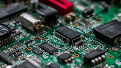
Quality Assurance in PCB Production: Testing and Validation Standards
Quality assurance is a critical component in PCB production, ensuring that each board meets the necessary performance and reliability standards. In the journey from design to assembly, testing and validation play pivotal roles in identifying defects and confirming that specifications are met. Techniques such as optical inspection, automated test equipment, and functional testing help to ensure that PCBs are free from manufacturing errors and operate as intended in their final applications.
**Tips:** When selecting testing methods, consider the complexity of your PCB design. For simpler designs, basic functional testing may suffice, whereas complex boards may require in-depth testing protocols, such as boundary scan and X-ray inspection, to verify hidden connections and solder joints. Additionally, ensure that your testing phases are well-documented to maintain compliance with industry standards and facilitate future audits.
Regular audits of the PCB assembly process also contribute significantly to quality assurance. By implementing standardized validation procedures throughout production, manufacturers can detect discrepancies early, minimizing risks and reducing waste. Consistent training for staff on quality control processes is essential to maintain high standards and reinforce a culture focused on quality.
**Tips:** Foster open communication between design engineers and production teams to address potential design flaws before assembly begins. Early collaboration can save time and resources by mitigating risks associated with late-stage design changes.
Quality Assurance in PCB Production: Testing and Validation Standards