Top 10 Tips for Effective PCB Board Design for Beginners and Experts
Designing a printed circuit board (PCB) is a crucial step in the development of any electronic device, whether you're an experienced engineer or a beginner. Effective PCB board design not only influences the performance and reliability of the final product but also impacts the manufacturing process and cost. This article aims to provide valuable insights for individuals at any skill level looking to enhance their PCB board design skills. By focusing on essential tips and best practices, we will guide you through the intricacies of PCB design to ensure that your projects succeed from both a technical and practical standpoint.
In today's fast-paced technological landscape, understanding the fundamentals of PCB board design is more important than ever. As devices become increasingly complex, the ability to create efficient and effective PCBs can set your project apart. Whether you are tackling simple circuit layouts or intricate designs, applying the right techniques and considerations can significantly improve your outcomes. This article will explore the top ten tips that cater to both novices and seasoned professionals, ensuring that everyone can benefit from the insights shared here. With a solid foundation in these essential principles, you will be well-equipped to tackle any PCB design challenge that comes your way.

Understanding the Basics of PCB Design Principles
Understanding the basics of PCB (Printed Circuit Board) design principles is crucial for both beginners and experts looking to create efficient and reliable electronic devices. A well-designed PCB forms the backbone of any electronic product, ensuring that the circuits function correctly while minimizing issues such as signal integrity and electromagnetic interference. According to a report by IPC, up to 50% of design revisions stem from layout mistakes, highlighting the importance of mastering fundamental design principles from the outset.
One effective tip for achieving better PCB design is to prioritize component placement strategically. By grouping related components and optimizing their spatial orientation, designers can significantly reduce trace lengths and potential noise issues. Additionally, incorporating proper grounding techniques is essential; implementing a solid ground plane can enhance performance and stability, ensuring that the PCB operates under varying conditions. A survey conducted by Cadence Design Systems revealed that designs utilizing these practices improved performance by around 30%, emphasizing the profound impact of adhering to basic principles.
Furthermore, employing proper routing techniques is equally important. Keeping signal traces as short as possible and using wider traces for high-current applications can enhance reliability and reduce resistance. According to a study from the IEEE, around 70% of PCB failures originate from poor routing and trace design. Therefore, mastering these foundational aspects not only contributes to effective PCB design but also lays the groundwork for innovative solutions in the evolving electronics landscape.
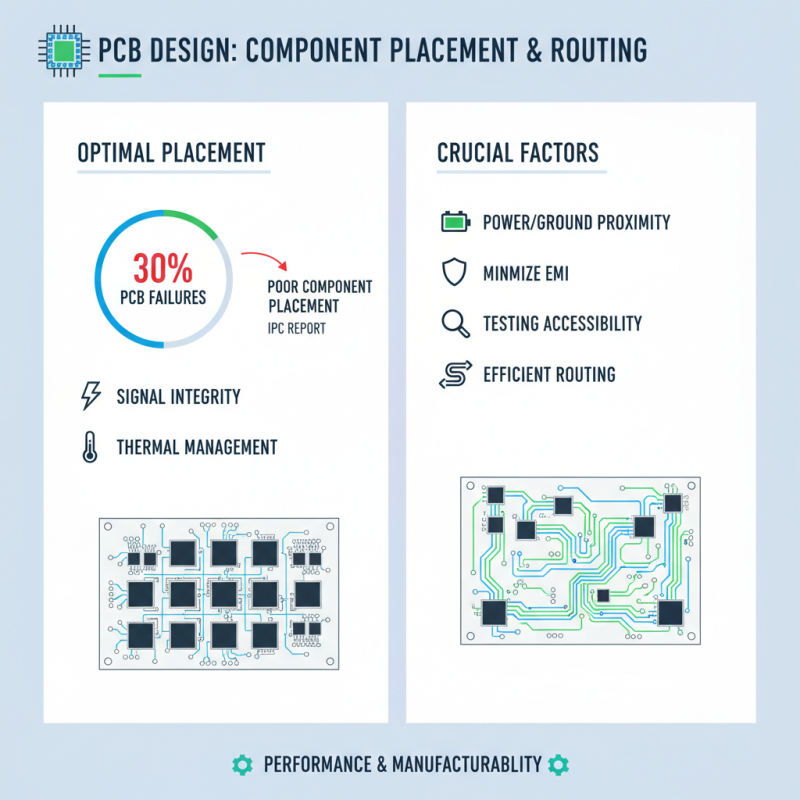
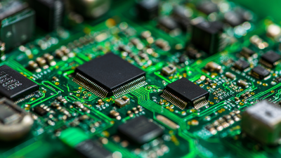
Key Considerations for Component Placement and Routing
When it comes to effective PCB board design, component placement and routing are crucial factors that influence both performance and manufacturability. According to a report by IPC, approximately 30% of PCB failures can be attributed to poor component placement, making it essential for designers to prioritize this aspect. Efficient component placement optimizes signal integrity and minimizes electromagnetic interference (EMI), crucial for high-frequency applications. Considerations such as proximity to power and ground paths, thermal management, and accessibility for testing should guide the arrangement of components on the board.
In terms of routing, designers must ensure that traces are efficiently laid out to reduce capacitance and inductance, thereby enhancing signal quality. The IPC-2221 standard emphasizes the importance of maintaining consistent trace width and spacing to adhere to electrical specifications, with variations potentially leading to increased resistance and overheating. Furthermore, utilizing vias judiciously can significantly influence the overall performance, as excessive via usage can degrade signal quality due to increased inductance and resistance. By following best practices in component placement and routing, designers can create PCBs that meet performance expectations while remaining cost-effective and reliable in various applications.
Utilizing Design Software Tools for Effective PCB Layout
When embarking on PCB design, leveraging the right design software tools is an essential step that can significantly impact the outcome of your project. Recent industry reports indicate that nearly 70% of PCB design inefficiencies stem from poor software utilization and lack of proficiency in advanced features. Beginners and experts alike can enhance their layouts by familiarizing themselves with features such as automated routing, design rule checks (DRC), and simulation capabilities. Incorporating these tools not only accelerates the design process but also minimizes costly errors that could arise during manufacturing.
One important tip for effective PCB layout is to prioritize component placement strategically. Effective software tools offer visualizations and design guidelines that help in positioning components to optimize signal integrity and reduce electromagnetic interference (EMI). The goal is to keep high-speed signals and power traces as short as possible while ensuring adequate grounding and decoupling. Additionally, utilize the software’s built-in functionalities to arrange traces efficiently. The ability to visualize signal flow and trace lengths can drastically reduce design iterations, improving both time management and product reliability.
Another recommendation is to take full advantage of simulation tools included within PCB design software. Simulations allow designers to test their layouts virtually for potential thermal and electrical issues before proceeding to production. According to PCB industry analyses, companies that implemented simulation tools reported a 30% decrease in design rework costs. By predicting performance and identifying flaws early, designers can make necessary adjustments, saving both time and resources while ensuring a robust final product.
Testing and Prototyping: Ensuring PCB Functionality and Reliability
Testing and prototyping are critical stages in the PCB design process, ensuring that a board functions correctly before mass production. According to a report by IPC, approximately 30% of PCB design failures can be attributed to inadequate testing and validation procedures. This statistic underscores the importance of implementing a robust testing strategy that includes electrical tests, thermal analysis, and signal integrity assessments. By utilizing advanced simulation tools in the prototyping phase, designers can preemptively identify potential issues, reducing costly revisions during manufacturing.
Moreover, the rapid advancement of PCB technology has led to the adoption of more sophisticated methodologies for prototyping, such as 3D printing and rapid prototyping techniques. These methods not only shorten the design cycle but also enhance the reliability of tests conducted on prototypes. A study by the IEEE Access found that utilizing these innovative approaches can cut down the typical prototyping time by up to 50%, enabling faster iterations and improved design outcomes. By leveraging comprehensive testing frameworks and modern prototyping techniques, both beginners and experts can ensure the functionality and reliability of their PCBs, ultimately leading to higher-quality end products.
Top 10 Tips for Effective PCB Board Design
Common Mistakes to Avoid in PCB Design for Optimal Results
When venturing into PCB (Printed Circuit Board) design, avoiding common pitfalls can significantly enhance both functionality and manufacturability. One primary mistake is neglecting proper component placement. Beginners often stack components too closely together, which can lead to heat dissipation issues or signal interference.
To prevent these problems, it's crucial to ensure ample spacing and logical layouts that consider the signal flow and thermal characteristics of the components.
Another frequent error is inadequate power distribution. Designers may overlook the importance of thickened traces or proper ground planes, which can cause voltage drops and affect performance. A comprehensive power distribution strategy that includes decoupling capacitors and well-planned trace widths will help maintain consistent voltage levels across the PCB.
By being mindful of these aspects, both novice and seasoned designers can create more reliable and efficient circuit boards, ultimately leading to better project outcomes.